Laminated construction boosts interface stability in inverted perovskite photo voltaic cells
by Simon Mansfield
Sydney, Australia (SPX) Could 05, 2025
A analysis partnership between the Hong Kong College of Science and Expertise (HKUST) and the Hong Kong Polytechnic College (PolyU) has led to the event of a laminated microstructure interface that considerably enhances the effectivity and stability of inverted perovskite photo voltaic cells.
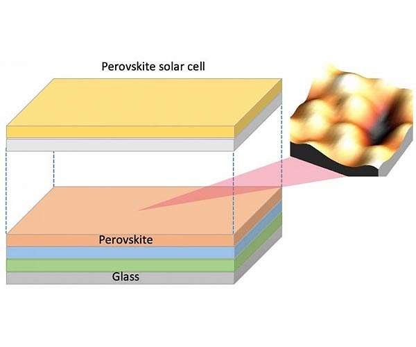
Perovskite photo voltaic cells are considered robust candidates to succeed silicon-based cells throughout purposes like transportable gadgets, grid programs, and aerospace applied sciences. Their enchantment lies of their excessive effectivity, low manufacturing value, and design flexibility. Amongst their configurations, inverted perovskite constructions provide improved materials stability. Nevertheless, these gadgets are nonetheless restricted by efficiency points associated to defect accumulation on the vital interface between the perovskite layer and the fullerene-based electron transport layer.
Led by Prof. Zhou Yuanyuan from HKUST’s Division of Chemical and Organic Engineering, and Prof. Cai Songhua of PolyU’s Division of Utilized Physics, the group centered on engineering a novel laminated interface. This interface contains three sequential layers: a molecular passivation layer, a fullerene by-product layer, and a two-dimensional perovskite layer. This tripartite construction considerably reduces defect density and improves power alignment between layers.
The improved interface ends in superior gadget efficiency and larger sturdiness beneath situations reminiscent of extended gentle publicity and excessive humidity. In response to Dr. Guo Pengfei, co-first creator and postdoctoral fellow at HKUST, “We launched the idea of composite supplies into the interface design of optoelectronic gadgets, permitting the synergistic results of every layer on this new interface to realize outcomes which are unattainable with conventional interface engineering.”
Prof. Zhou emphasised the significance of understanding materials habits on the micro and atomic ranges. “Perovskite is a gentle lattice materials. We will create microstructural options in this sort of materials which are tough to realize with standard supplies. Our purpose is to know the formation and mechanisms of those microstructures on the nanoscale, and even on the atomic scale, to drive gadget innovation primarily based on this elementary understanding.”
Analysis Report:Synthesis of a lattice-resolved laminate-structured perovskite heterointerface
Associated Hyperlinks
Hong Kong University of Science and Technology
All About Solar Energy at SolarDaily.com
Trending Merchandise