by Robert Schreiber
Berlin, Germany (SPX) Feb 18, 2026
Regardless of being riddled with impurities and defects, answer processed lead halide perovskites proceed to defy expectations as extremely environment friendly photo voltaic cell supplies, with efficiency now approaching that of trade customary silicon based mostly gadgets. A brand new experimental research from the Institute of Science and Expertise Austria (ISTA) affords a complete bodily rationalization for this effectivity puzzle and factors the way in which to more practical subsequent era photovoltaic applied sciences.
Over the previous 15 years, lead halide perovskites have risen from relative obscurity to grow to be main candidates for low price, excessive efficiency photo voltaic cells. Initially catalogued within the Nineteen Seventies for his or her hybrid natural inorganic crystal constructions after which largely forgotten, these compounds had been rediscovered within the early 2010s when researchers discovered that they exhibit distinctive photovoltaic conduct in addition to sturdy efficiency in mild emitting diodes and X ray detection and imaging.
Perovskites additionally show hanging quantum mechanical properties, together with quantum coherence at room temperature, making them engaging testbeds for advanced condensed matter physics. But their sensible promise has been shadowed by a primary paradox. Not like silicon photo voltaic cells, which depend on extremely pure, rigorously grown single crystal wafers to attenuate defects, perovskite gadgets are usually made utilizing cheap answer based mostly processes that depart them crammed with structural imperfections.
In typical silicon expertise, such defects are rigorously eradicated as a result of they entice cost carriers and forestall them from traversing the a whole lot of microns required to succeed in the electrodes and generate helpful present. The query for perovskites has due to this fact been how electrons and holes handle to maneuver over lengthy distances and survive for lengthy instances in a fabric that, by customary standards, ought to be riddled with traps and recombination facilities.
ISTA postdoctoral researcher Dmytro Rak and assistant professor Zhanybek Alpichshev tackled this downside by specializing in how expenses behave inside the majority of a perovskite crystal. Earlier research had proven that when electrons and holes type tightly certain excitons in these supplies, they usually recombine quickly. Nonetheless, experiments additionally indicated that in working gadgets the fees usually stay separated for prolonged intervals, an obvious contradiction that instructed some inner power should be performing to drag the pairs aside.
To probe this concept, the staff used nonlinear optical strategies to inject electrons and holes deep inside single crystal perovskite samples after which monitored the ensuing electrical response. Every time they generated a contemporary inhabitants of expenses, they detected a finite present flowing in the identical course via the fabric despite the fact that no exterior voltage was utilized. This conduct pointed to inbuilt inner fields able to separating reverse expenses nicely away from the electrodes.
Nonetheless, customary characterizations of the intrinsic crystal construction of lead halide perovskites had indicated that such bulk photovoltaic results shouldn’t be current uniformly all through the fabric. Rak and Alpichshev proposed as a substitute that the essential fields reside at area partitions, skinny areas of modified construction that type a microscopic community extending via the crystal. At these partitions, native distortions might break the symmetry and create sturdy inner electrical fields.
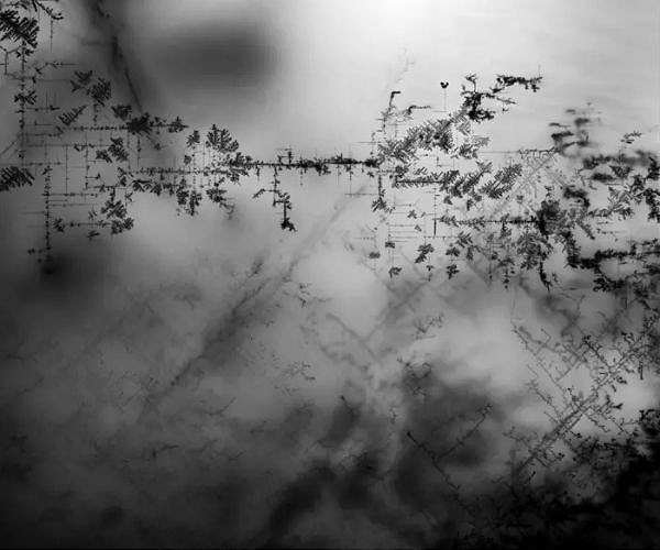
Visualizing such a website wall community deep inside a crystal posed a significant experimental problem, as a result of many frequent probes are delicate primarily to the floor the place properties can differ from the majority. Drawing on his chemistry background, Rak devised an electrochemical staining methodology that makes use of ionic conduction within the perovskite to focus on the interior construction. He allowed silver ions to diffuse into the crystal the place they preferentially accrued at area partitions, then transformed the ions into metallic silver in order that the ensuing filaments could possibly be imaged with optical microscopy.
The ensuing footage revealed a dense, pattern spanning community of silver enriched paths that hint the area wall skeleton of the crystal. Alpichshev likens the strategy to angiography in dwelling tissue, however utilized to the microstructure of a strong, as a result of it exposes the interior channels alongside which expenses can transfer. The qualitative method, invented and carried out at ISTA, offers direct proof that perovskites host intricate inner architectures quite than being uniformly disordered.
Rak and colleagues interpret these area partitions as pure highways for cost carriers. When mild absorption creates an electron gap pair close to one among these partitions, the native electrical area pulls the negatively charged electron and the positively charged gap to reverse sides, stopping fast recombination. As soon as separated, the carriers can drift alongside the prolonged area wall community for distances that may be extraordinary on a microscopic timescale, ultimately reaching the electrodes and contributing to the present.
On this image, the very defects that may be detrimental in a standard semiconductor grow to be useful parts that allow environment friendly power harvesting. As a substitute of striving for defect free crystals, perovskite expertise advantages from the presence and connectivity of flexoelectric area partitions that crisscross the majority and maintain lengthy vary cost transport below illumination.
The authors argue that their framework reconciles a spread of beforehand conflicting experimental observations on lead halide perovskites, together with fast exciton recombination in some measurements and lengthy service lifetimes and diffusion lengths in others. By emphasizing the position of inner fields and area wall networks, their mannequin affords a unified understanding of how these supplies obtain excessive energy conversion efficiencies regardless of obvious structural dysfunction.
Thus far, a lot of the analysis effort in perovskite photovoltaics has centered on adjusting chemical composition to enhance stability and efficiency, usually with solely incremental positive aspects. The ISTA findings counsel a complementary path that focuses on engineering the density, orientation and connectivity of area partitions to optimize cost separation and transport whereas preserving the answer based mostly, low price fabrication routes that make perovskites engaging for giant scale deployment.
Analysis Report:Flexoelectric domain walls enable charge separation and transport in cubic perovskites
Associated Hyperlinks
Alpichshev Group at Institute of Science and Technology Austria
All About Solar Energy at SolarDaily.com
Trending Merchandise