by Riko Seibo
Tokyo, Japan (SPX) Jan 03, 2026
Perovskite photo voltaic cells are attracting curiosity as lower-cost, high-efficiency alternate options to silicon photovoltaics, however defects of their skinny movies hinder cost transport, waste vitality, and cut back system stability.
One method to mitigate these defects is passivation remedy, by which easy salts or natural molecules are launched into the perovskite movie in order that small molecules or ions bind to defect websites and restrict their affect on electrical conduction. Nonetheless, most present characterization strategies solely probe the movie floor or present averaged macroscopic measurements, making it troublesome to substantiate how effectively completely different passivation methods work contained in the movie quantity.
Researchers on the Ningbo Institute of Supplies Expertise and Engineering (NIMTE) of the Chinese language Academy of Sciences have now developed a three-dimensional electrical imaging technique that immediately visualizes how defect passivation operates inside perovskite layers. The examine, printed on December 31 within the journal Newton, studies that this technique can map cost transport all through the movie and hyperlink these microscopic options to photo voltaic cell efficiency.
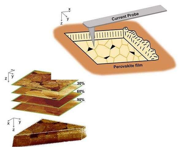
The method depends on tomographic conductive atomic pressure microscopy, or TC-AFM, which measures native electrical conductivity whereas the instrument sequentially removes ultrathin layers from the perovskite movie. By stacking the conductivity information acquired at every depth, the group reconstructs a three-dimensional map of present distribution and cost transport pathways with nanoscale spatial decision.
Utilizing TC-AFM, the researchers in contrast perovskite movies processed with completely different passivation methods and immediately noticed modifications of their inside electrical conduct. Movies with out passivation confirmed widespread low-conductivity areas that impede cost movement, whereas bulk passivation lowered these resistive domains throughout the movie, particularly alongside grain boundaries.
Floor passivation produced a unique profile, primarily enhancing conductivity close to the highest interface of the movie, which is vital for integration into full system architectures. When each bulk and floor passivation had been utilized collectively, the movies displayed essentially the most uniform and steady conductive networks, with the remaining low-conductivity zones largely restricted to the floor.
“These microscopic electrical traits are intently correlated with the ensuing photo voltaic cell efficiency, establishing a direct hyperlink between 3D cost transport throughout the movie and general system effectivity,” famous Prof. XIAO Chuanxiao, a corresponding creator of the examine.
By delivering a direct three-dimensional view of charge-carrier migration in perovskite layers, the brand new technique gives a device for assessing and refining passivation methods. The authors report that this method can information the rational design of higher-quality perovskite supplies and help the event of extra environment friendly and secure perovskite photo voltaic cells, in addition to different thin-film digital and optoelectronic units.
Analysis Report:Three-dimensional mapping of electrical behavior in perovskite films using tomographic conductive atomic force microscopy
Associated Hyperlinks
Ningbo Institute of Materials Technology and Engineering, Chinese Academy of Sciences
All About Solar Energy at SolarDaily.com
Trending Merchandise