by Sarah Collins
Cambridge UK (SPX) Nov 14, 2025
Researchers have achieved a brand new degree of management over the atomic construction of a household of supplies generally known as halide perovskites, making a finely tuned ‘vitality sandwich’ that would remodel how photo voltaic cells, LEDs and lasers are made.
Because of their exceptional skill to soak up and emit mild, and since they’re cheaper and may be configured to transform extra of the photo voltaic spectrum into vitality than silicon, perovskites have lengthy been touted as a possible alternative for silicon in photo voltaic cells, LEDs and quantum applied sciences.
Nonetheless, their instability and sturdiness has, up to now, largely restricted perovskite gadgets to the laboratory. As well as, scientists have struggled to exactly management the thickness of perovskite movies, and management how totally different perovskite layers work together when stacked collectively – an necessary step in constructing practical, multi-layered buildings.
Now, a group of researchers led by the College of Cambridge has discovered a brand new method to develop ultra-thin layers of perovskite movies so their atoms line up completely, which might allow extra highly effective, sturdy and environment friendly gadgets.
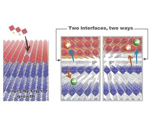
The researchers used a vapour-based method to develop three-dimensional and two-dimensional perovskites one layer at a time, which enabled them to regulate the thicknesses of the movies all the way down to fractions of an atom. Their outcomes, reported within the journal Science, might open the door to usable perovskite gadgets that may be produced at scale, utilizing a course of like that used to make business semiconductors.
Every layer in a semiconductor ‘sandwich’ does a special job in shifting electrons and their positively-charged counterparts – referred to as holes – round and determines how the semiconductors take up or emit mild. Collectively, the layers act like one-way streets that information the electrical costs in reverse instructions, stopping them from bumping again into one another and losing vitality as warmth.
In different widely-used semiconductors, equivalent to silicon or newer supplies equivalent to gallium nitride, the properties of the person layers may be fine-tuned utilizing numerous strategies. However perovskites, regardless of their wonderful efficiency, have up to now proved tough to regulate in layered gadgets, due partly to their ‘chaotic’ atomic construction.
“A variety of perovskite analysis makes use of resolution processing, which is messy and exhausting to regulate,” Professor Sam Stranks from the Division of Chemical Engineering and Biotechnology, who co-led the analysis. “By switching to vapour processing – the identical technique used for traditional semiconductors – we are able to get that very same diploma of atomic management, however with supplies which can be way more forgiving.”
The researchers used a mix of three-dimensional and two-dimensional perovskites to create and management their atomically-tuned stacks, a phenomenon generally known as epitaxial progress. This effective management let the group instantly observe how the sunshine given off by the fabric adjustments relying on whether or not it is a single layer, a double layer, or thicker.
“The hope was we might develop an ideal perovskite crystal the place we alter the chemical composition layer by layer, and that is what we did,” stated co-first creator Dr Yang Lu from Cambridge’s Division of Chemical Engineering and Biotechnology and Cavendish Laboratory. “It is like constructing a semiconductor from the bottom up, one atomic layer after one other, however with supplies which can be a lot simpler and cheaper to course of.”
The researchers additionally discovered they might engineer the junctions between the layers to regulate whether or not electrons and holes stayed collectively or aside – a key consider how effectively a fabric emits mild.
“We have reached a degree of tunability that wasn’t even on our radar after we began,” stated Professor Sir Richard Buddy from the Cavendish Laboratory, who co-led the analysis. “We are able to now resolve what sort of junction we would like – one which holds costs collectively or one which pulls them aside – simply by barely altering the expansion situations.”
The researchers discovered they might tune the vitality distinction between the layers by greater than half an electron volt, and in some circumstances, prolong the lifetime of electrons and holes to over 10 microseconds: far longer than common.
The group says this degree of precision might pave the way in which for scalable, high-performance gadgets that use mild in new methods, from lasers and detectors to next-generation quantum applied sciences.
“Altering the composition and efficiency of perovskites at will – and probing these adjustments – is an actual achievement and displays the period of time and funding we have made right here at Cambridge,” stated Stranks. “However extra importantly, it exhibits how we are able to make working semiconductors from perovskites, which might someday revolutionise how we make low-cost electronics and photo voltaic cells.”
The analysis was supported partly by the Royal Society, the European Analysis Council, the Simons Basis, and the Engineering and Bodily Sciences Analysis Council (EPSRC), a part of UK Analysis and Innovation (UKRI). Richard Buddy is a Fellow of St John’s Faculty, Cambridge. Sam Stranks is a Fellow of Clare Faculty, Cambridge.
Analysis Report:Layer-by-layer epitaxial growth of perovskite heterostructures with tunable band offsets
Associated Hyperlinks
University of Cambridge
All About Solar Energy at SolarDaily.com
Trending Merchandise